GPT-Synopsys Combines IC Design EDA with Agentic AI

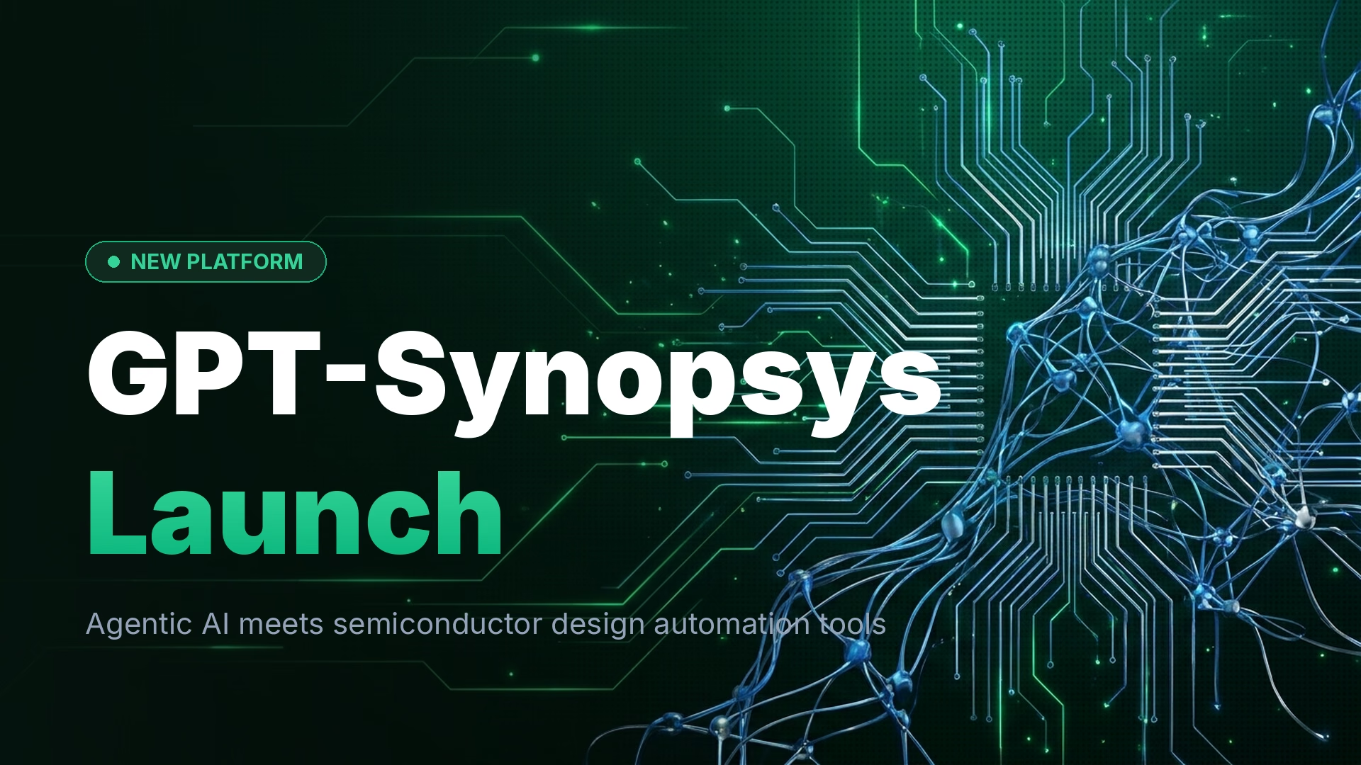
Synopsys has unveiled GPT-Synopsys, a specialized agentic AI platform designed to automate integrated circuit design workflows by integrating directly with Electronic Design Automation (EDA) tools. Officially launched on November 4, 2026, the platform represents a significant evolution in semiconductor engineering, enabling AI agents to independently execute complex chip design tasks that traditionally required extensive human oversight and manual tool orchestration.
Platform Architecture and EDA Integration
GPT-Synopsys operates as an agentic AI system with deep hooks into Synopsys' suite of semiconductor design software. The platform interprets natural language design specifications, translates them into actionable workflows, and autonomously navigates EDA tools to complete tasks ranging from physical verification to power optimization. Unlike general-purpose coding assistants, GPT-Synopsys understands domain-specific constraints like timing closure, design rule checks, and manufacturing tolerances inherent to silicon engineering.
The system employs an agentic workflow architecture that allows multiple specialized agents to collaborate on different aspects of IC design. One agent might handle floorplanning while another optimizes signal integrity, with a coordinating layer ensuring design coherence across parallel operations. This multi-agent approach mirrors how experienced engineering teams distribute chip design responsibilities, but operates at machine speed with continuous context awareness.
Target Applications and Use Cases
Hardware engineers can deploy GPT-Synopsys for repetitive design validation tasks, automated regression testing of design changes, and exploratory architecture optimization. The platform excels at scenarios requiring iterative refinement, such as adjusting transistor sizing to meet power budgets or re-routing critical nets to eliminate timing violations. Early adopters report significant reductions in time spent on mechanical design iterations, allowing human engineers to focus on creative problem-solving and architectural decisions.
- Automated physical verification and DRC cleanup across multiple process nodes
- Autonomous power-performance-area (PPA) optimization using reinforcement learning techniques
- Natural language querying of design databases for anomaly detection and constraint violations
Competitive Landscape and Industry Context
The launch positions Synopsys directly alongside other AI-enhanced semiconductor design tools emerging in 2026. While competitors have introduced machine learning models for specific EDA subtasks, GPT-Synopsys distinguishes itself through end-to-end workflow automation and its ability to reason across the full design stack. The platform's integration with Synopsys' established toolchain provides immediate production readiness for existing customers, reducing the adoption friction typically associated with new AI infrastructure.
Industry analysts note that agentic AI in semiconductor design addresses a critical bottleneck as chip complexity outpaces available engineering talent. With leading-edge processes requiring verification of billions of transistors and compliance with thousands of design rules, autonomous agents capable of managing this complexity represent a structural shift in how silicon gets designed. GPT-Synopsys' ability to ingest legacy design knowledge and apply it to new projects could accelerate development cycles by months.
Availability and Deployment Model
Officially released on November 4, 2026, GPT-Synopsys is available to Synopsys EDA customers through both cloud-based and on-premises deployment options. The platform requires integration with existing Synopsys tool licenses and operates as an orchestration layer rather than a replacement for established design software. Pricing follows a consumption-based model tied to compute resources and agent task complexity, with enterprise licensing available for high-volume design organizations.
What This Means
GPT-Synopsys marks a pivotal moment in semiconductor engineering, demonstrating that agentic AI can handle the precision and complexity demands of physical chip design. For hardware teams facing aggressive tape-out schedules, the platform offers a force multiplier that automates grunt work without sacrificing design quality. As AI agents become fluent in EDA tool operation, the traditional boundaries between software and hardware engineering may blur, with natural language specifications increasingly replacing manual tool manipulation as the primary interface for silicon creation.


on Emergent today